Coreless工艺
Coreless Process
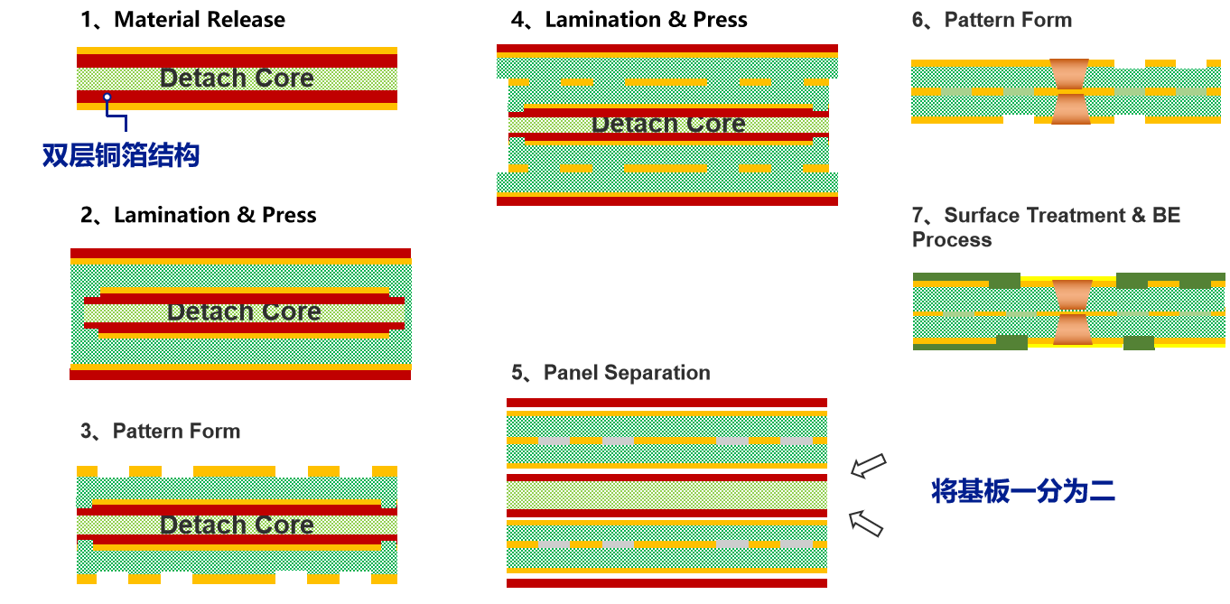
利用双层铜箔结构的Detach Core为芯板,通过增层工艺形成多层板;在将Detach Core的双层铜箔分开,Detach Core拆解掉,基板一分为二,变为两枚基板。利用该工艺制作的无芯板,板厚可以做到极薄,也能加工奇数层结构。
Coreless工艺在基板厚度空间要求苛刻的场景使用广泛,其生产工艺过程如下:
Using a“Detach Core”which has two-layers carrier foil structure on the surface as a core, and forming a multilayer board by lamination Process. Delamination the board by separating from the two-layers carrier foil, removing the “detach Core”, and splitting in two boards without core, which call “coreless”. Extremely thin board and odd-layers structures can be formed by this coreless process.
Coreless process is widely used in applications where thin board thickness requirement, and the process is as follows:
ETS工艺
ETS Process
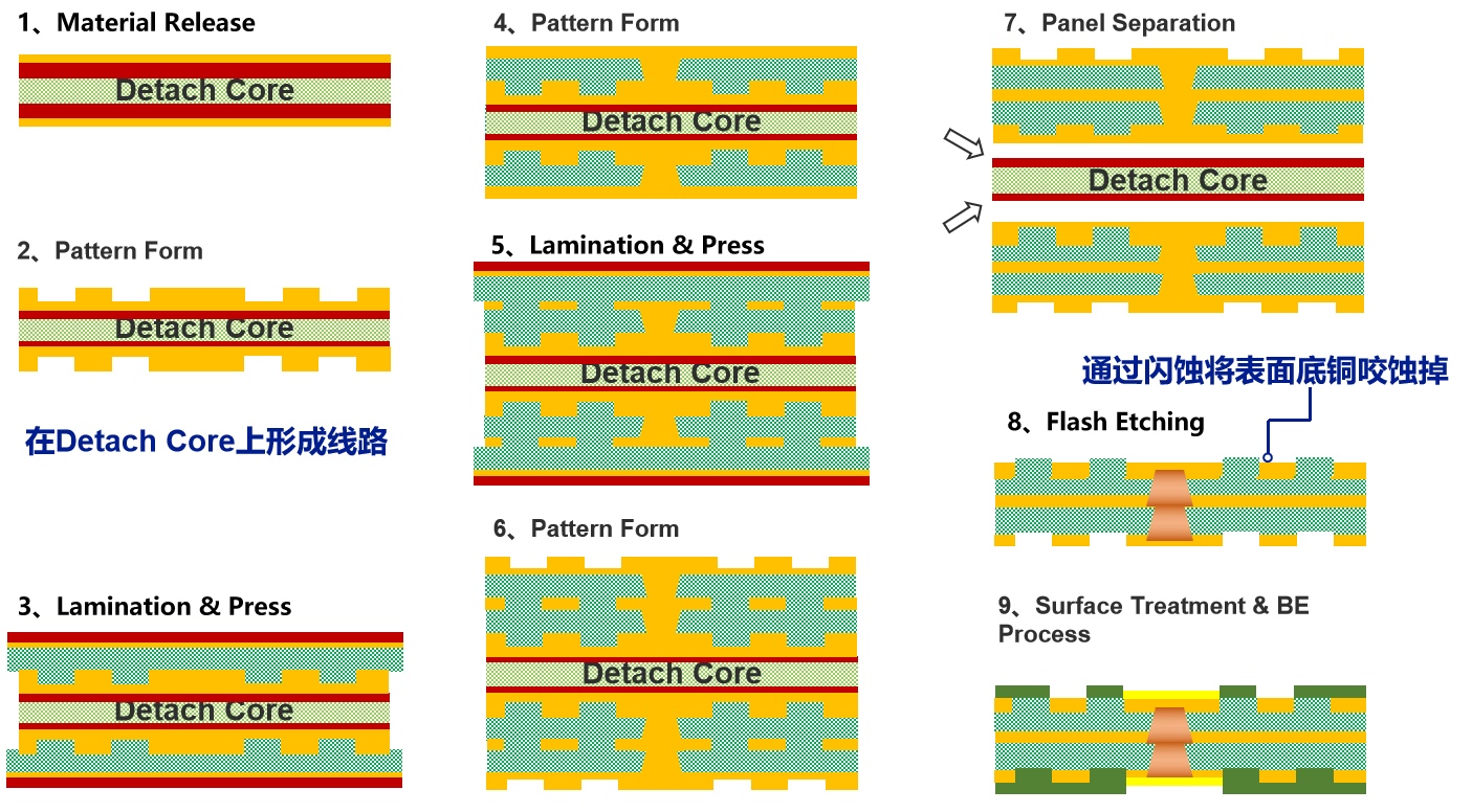
ETS工艺全称为Embedded Trace Substrate,其工艺也是一种Coreless工艺,区别在于:有一层表层线路形成在Detach Core材料的表层铜箔上,并利用压合工艺将线路埋入介质层中(而Coreless工艺是直接在铜箔上增层);再在基板分离后,通过闪蚀将底铜咬蚀掉形成埋入式图形。
ETS工艺用在空间要求苛刻、且I/O数密集的场景,如存储芯片,其生产工艺过程如下:
ETS(Embedded Trace Substrate) process, is a kind of coreless process, the difference is: There is a the circuits pattern layer formed on the surface copper foil of detach core, and then laminating prepreg on the circuits pattern layer which the fine trace is embedded in the dielectrics; separating the multi-layer board to two boards; removing the surface copper by etching and forming a “Embedded Trace”Layer finally.
The ETS substrate is used in extremely high intensive I/O count applications, such as memory chips, and the process is as follows: