

FCBGA载板FCBGA Substrate产品介绍Product Introduction 产品一般采用胶膜增层(Build-up Film Lamination)工艺,线路形成使用半加成(SAP)工艺。代表产品有倒装芯片封装形式的FCBGA(Flip Chip Ball Grid Array)封装载板。 该类产品特点:大尺寸、高多层、高密度;用于大算力(HPC)的应用,如GPU、CPU、FPGA、AI计算、5G/6G等场景。 The substrates stack up with Build-up Film(such as ABF,Ajinomoto Build-up Film),and the circuits form by Semi-Add Process(SAP). Representative application such as FCBGA packaging by Flip Chip. The characteristics of this kind of substrates: large unit size、high layer counts、high density interconnecting, Applying to High Performance Computing(HPC) applications, such as GPU, CPU, FPGA, AI, 5G/6G. | 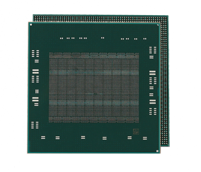 |
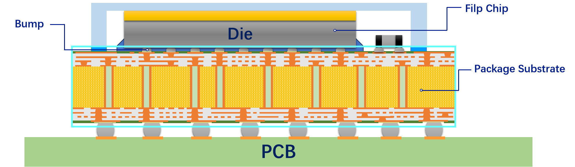
封装示意图Package Structure
产品特征Features
最新一代激光打孔设备加工更小的微孔
Smaller micro via by new-generation laser drilling machine
加成工艺实现更细的线路/间距
Fine Line/Space by SAP process
高多层
Multi-Layer
大尺寸
Large Unit Size
高密度
High Density
产品结构Build-up Structure

特征规格Process Capability
- 层数:6~20层
- 板厚: 0.2~2.0mm
- 线宽/间距=9/12μm
- 微孔/焊盘=Φ55/85μm
- 通孔上叠微孔(POFV)
- 阻焊开窗: Φ60μm
- 阻焊对位: ±12.5μm
- 表面完工: 化锡、镍钯金、OSP
- 植球凸点(Micro Bump) Pitch: 110μm
- Layer Count: 6~20
- Board Thickness: 0.2~2.0mm
- Line/Space=9/12μm
- Via/Land=Φ55/85μm
- POFV(Plating over Filled Via, Via on through hole)
- SRO: Φ60μm
- SRO/Land Reg.: ±12.5μm
- Surface Finish: IT、ENEPIG、OSP
- Micro bump Pitch:110μm
应用Applications
- CPU、MPU
- GPU
- ASIC
- FPGA
- AI
- 5G


