mSAP工艺
mSAP Process
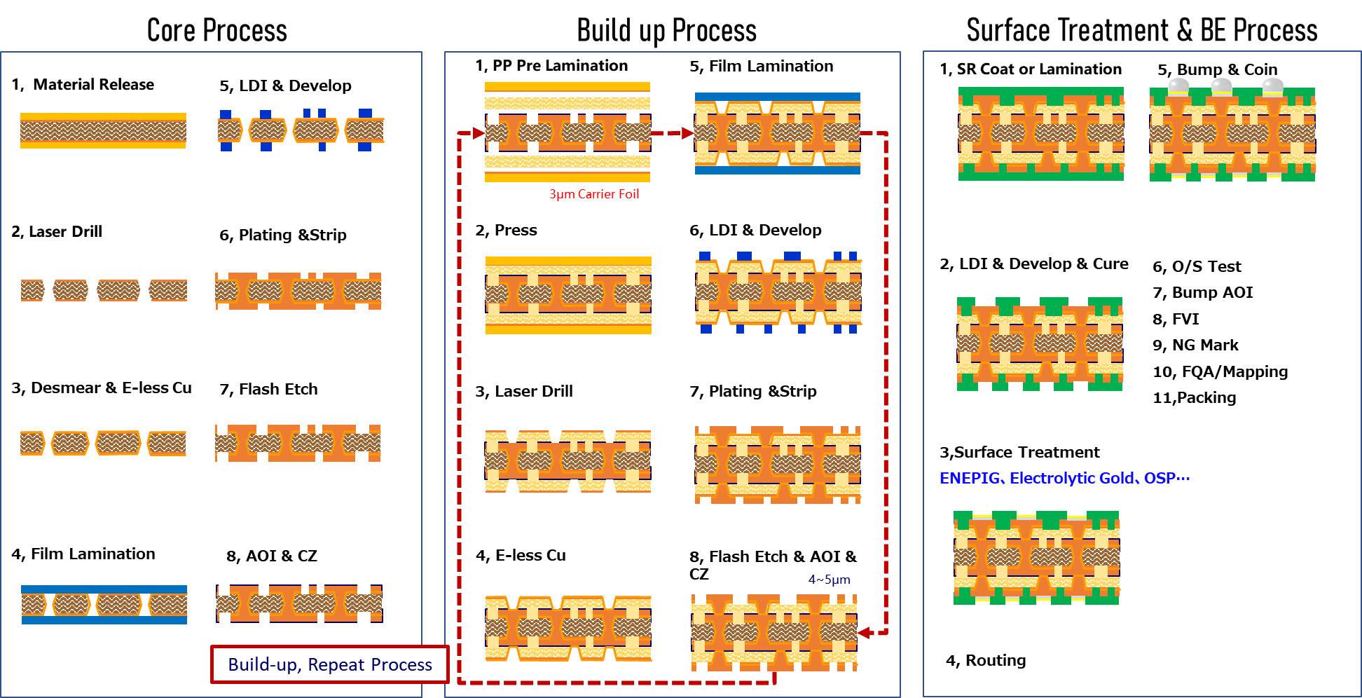
全称Modified Semi-Added Process,该工艺用在载板的芯板层或压合增层上,其工艺是通过压合工艺在介质材料上形成一层超薄铜箔,首先在铜箔上沉积一层种子铜,起到导电功能;然后在表面贴敷上感光胶膜,通过图形转移技术,形成感光膜图形;再进行图形金属化技术形成线路;最后闪蚀除去图形间种子铜和底铜。 mSAP工艺是在SAP工艺上进行的工艺改进,降低了种子铜形成的技术难度,但闪蚀时需要去除种子铜和底铜,对线路咬蚀量大一些,精细线路的形成能力也有下降。
mSAP工艺使用的材料通常有玻璃纤维增强,CTE较小,适合轻薄、器件空间限制的场景,其生产工艺过程如下:
Modified Semi-Added Process abbreviated as mSAP, which can be used on the core or build-up layers, pattern forming as follow: Laminating ultra thin copper foil with the dielectric material(such as prepreg) by pressing; Depositing with a very thin copper seed on the surface and in micro vias as a conductive layer; Laminating photosensitive dry film resist on the surface; forming the circuits pattern by the dry film using graphic transfer technology; and then metalizing with copper by filling the spaces of the dry film pattern; Removing copper seeds between metalizing copper patterns by flash-etching and firming the copper circuits finally. The mSAP process is improved from SAP process, which is easier than SAP as copper seed is much easier deposited on the copper foil than on the build-up film. But more etching is needed to removed copper seed layer and copper foil between patterns, which also more etching on metalizing copper patterns. The capability of fine line/space forming of mSAP is less than SAP.
The stack-up materials in the mSAP process usually have glass fiber reinforcement with low CTE, such as BT based or equivalent, which is suitable for thin and light devices. The process is as follows: