

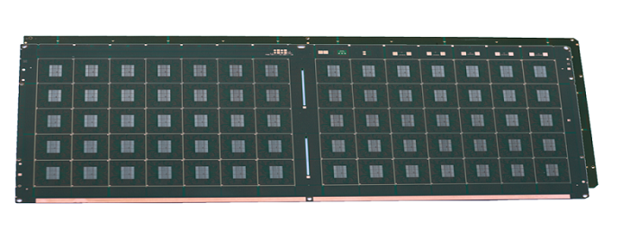
FCCSP载板FCCSP Substrate产品介绍Product Introduction 产品一般采用半固化片(Prepreg)压合增层(Pressing)的叠层工艺,线路形成使用改进型半加成(amSAP)工艺或减法(Tenting)工艺。代表产品有倒装芯片封装形式的FCCSP(Flip Chip Chip Scale Package)封装载板。 该类产品特点:尺寸小、轻薄、层数相对较少;用于穿戴、存储、射频等领域。 The product generally adopts the pressing lamination process of semi-curing sheets , and line formation uses an improved semi-additive (amSAP) process or subtraction (Tenting) process. The FCCSP (Flip Chip Chip Scale Package) package board in the form of inverted chip packaging for the product. The features of this type of product include small size, light weight, and relatively fewer layers. They are used in wearable, storage, and RF (radio frequency) applications. |
|
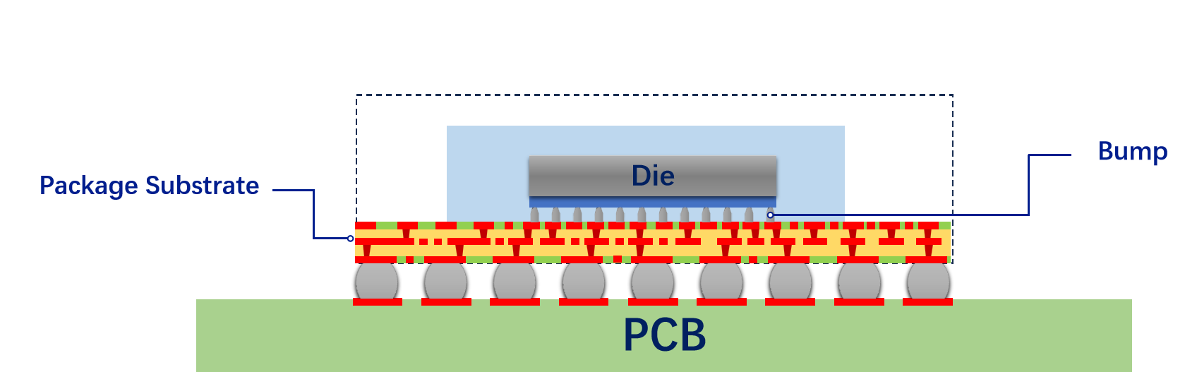
封装示意图Package Structure
产品特征Features
最新一代激光打孔设备加工更小的微孔
Smaller micro via by new-generation laser drilling machine
AMSAP工艺实现更细的线路/间距
Fine Line/Space by amSAP process
无芯板、ETS板
Ultra thin board by Coreless or ETS Process
薄板
Thin Thickness
小尺寸
Small size
高密度
High Density
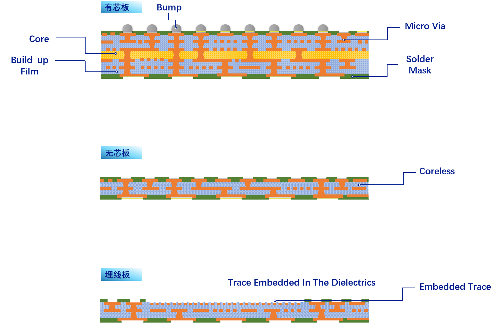
产品结构Build-up Structure
特征规格Process Capability
- Cored:
- 层数:2~8层 SiP :4~16层
- 板厚: 0.15~2.0mm
- amSAP工艺线宽/间距=15/15μm
- Tenting工艺线宽/间距=40/40μm
- 微孔/焊盘=Φ55/85μm
- 阻焊开窗: Φ:60μm
- 阻焊对位: ±12.5μm
- 表面完工: 镍钯金、OSP、部分镍钯金+OSP
- 植球凸点(Micro Bump) Pitch: 110μm
- Coreless:(2025H1)
- 层数:3~11层
- 板厚: 0.1~1.0mm
- ETS:(2025H1)
- 层数: 2~4层
- 板厚: 0.10~0.25mm
- 线宽/线距=10/10μm
- Cored:
- Layer Count: 2~8 SiP 4~16层
- Board Thickness: 0.15~2.0mm
- amSAP Line/Space=15/15μm
- Tenting Line/Space=40/40μm
- Via/Land=Φ55/85μm
- SRO: Φ60μm
- SRO/Land Reg.: ±12.5μm
- Surface Finish: ENEPIG、OSP、ENEPIG+OSP
- Micro bump Pitch:110μm
- Coreless:(2025H1)
- Layer Count: 3~11
- Board Thickness: 0.10~1.0mm
- ETS:(2025H1)
- Layer Count: 2~4
- Board Thickness: 0.10~0.25mm
- Line/Space:10/10μm
应用Applications
- AP
- BB
- RF
- PMIC
- Memory
- MEMS & Sensor
- Wearable


