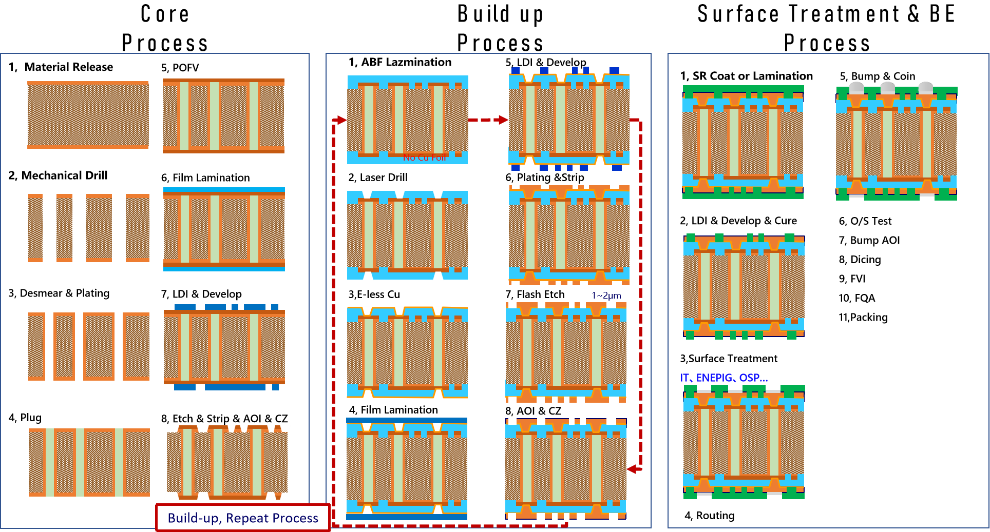
SAP工艺
SAP Process
全称Semi-Added Process,该工艺用在载板的增层膜(Build-up Film)上,其工艺是首先在材料增层胶膜(Build-up Film)上沉积一层种子铜,起到导电功能;然后在表面贴敷上感光胶膜(Photosensitive Dry Film Resist),通过图形转移技术,形成感光膜图形;再进行图形金属化技术形成线路;最后闪蚀除去图形间的种子铜。
SAP工艺技术难度较高,其生产工艺过程如下:
Semi-Added Process abbreviated as SAP, using on the build-up-layer pattern forming as follow:First depositing with a very thin copper seed on build-up film and in micro vias as a conductive layer; Laminating photosensitive dry film resist on the surface; forming the circuits pattern on the dry film using graphic transfer technology(exposure and development); and then metalizing with copper by filling the spaces of dry film pattern; Removing copper seeds between metalizing copper patterns by flash-etching and forming the copper circuits finally.
Compared with other conventional process, SAP Process needs higher level technology control. The process is as follows: